With the rapid development of electronic information, the amount of chips, liquid crystal displays and PCBs has increased significantly, especially the PCB industry is developing in a more and more refined direction. Among them, the most important processes are lithography and exposure.

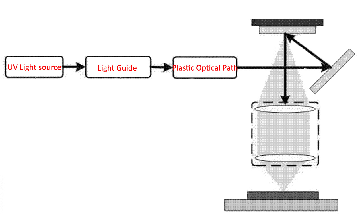
At present, the traditional exposure machine using film printing has a bottleneck, and the industry is more and more urgent for the laser direct imaging system (LDI). LDI systems often use DMD projection technology. The DMD is a square spatial modulator. In order to meet mass production, the light source must be irradiated on the DMD through a shaping system.

At present, laser shaping systems mostly use Koehler illumination system, free-form surface system or microlens array system. Koehler illumination adopts diaphragm modulation, which has low light energy utilization rate and poor uniformity modulation capability; free-form surface system is used to realize square shape. The uniform light spot has a very complex surface shape and is difficult to process; the microlens array system can well achieve a uniform light spot, but the light path is long and requires filter processing, which is not conducive to the lightweight of the imaging module. The imaging module can only expose a small part at a time, and for large-area exposure, it is necessary to implement scanning and stitching processing. Therefore, simplifying the imaging module will have a great effect on its assembly and precise motion control.
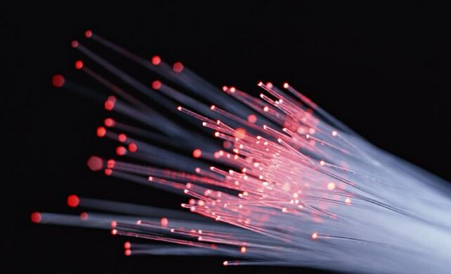
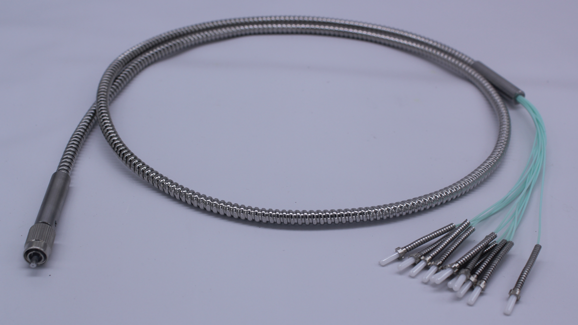
Nanjing Hecho Technology provide the Fiber Optic for LDI application, use high transmission efficiency low lose quartz Fiber Optic, customized service is available to meet the needs of different customers differenet requirements.
