Let the light change life

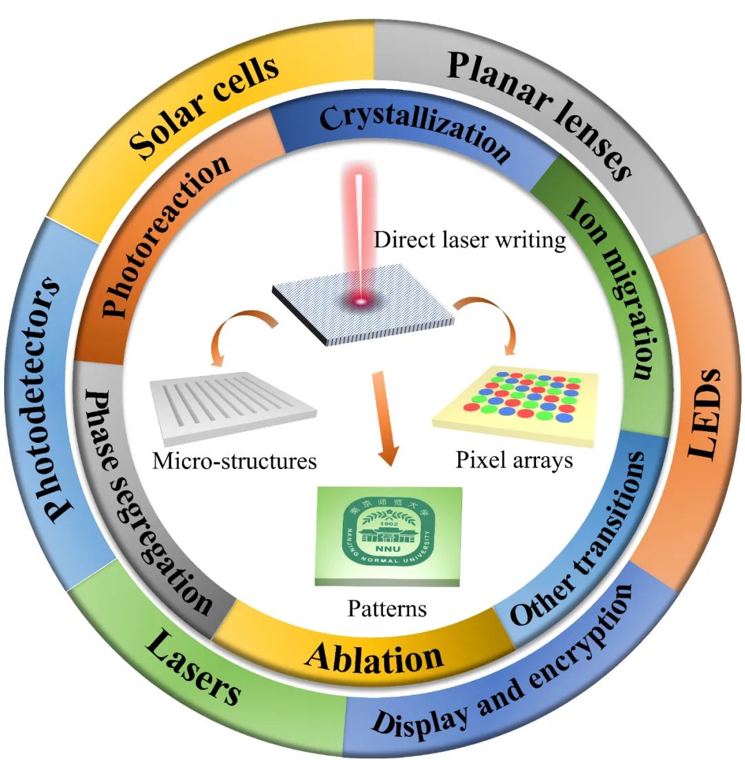
Metal halide perovskite has excellent photoelectric performance, and has become a well-deserved "star" material in the semiconductor field, and has attracted great attention from academia and industry. With the investment of a lot of research, the application of perovskite covers various fields such as single photon source, micro-nano laser, photodetector, optical logic gate, optical logic gates, optical communication, waveguide, nonlinear optics and other optical and optoelectronic fields. Therefore, the construction and integration of photonic devices with different functions based on a single perovskite chip is very promising.
The development of micro-nano processing technology is a key step in integrating various optoelectronic devices into a single chip to meet the requirements of advanced integrated optics, and will play a key role in the development of the next generation of information technology.
The laser direct writing (DLW) is an efficient, non-contact and mask-free micro-nano processing technology. It couples the laser beam with the microscope to reduce the size of the output spot and achieve high-resolution micro-nano processing. Depending on the manufacturing mechanism and the threshold response of the material, the DLW optimal resolution is usually between a few and several hundred nanometers. At the same time, DLW can flexibly manufacture any micro-nano structures on the same substrate, or it can use the spatial light modulator to change the focused laser field into a specific shape or produce multiple foci simultaneously, so as to meet the needs of large-scale manufacturing.
Mechanism of the interaction between laser light and perovskite
With the unique advantages of high precision, no contact, easy operation and no mask, laser is an excellent tool for the operation, fabrication and processing of micro-nano structures on semiconductors. The specific interaction mechanism between laser and perovskite can be divided into various phenomena, such as laser ablation, laser-induced crystallization, laser-induced ion migration, laser-induced phase separation, laser-induced light reaction and other laser-induced transitions. These different mechanisms of action represent different changes in perovskite crystals. For example, laser induced crystallization process is the nucleation and crystallization process of perovskite precursor, and laser induced phase separation is the separation of mixed phase perovskite into two different phases, both of which contain rich physical phenomena. The implementation of the whole micro-nano processing process is affected by the DLW parameters, such as wavelength, pulse / continuous wave, action time, power, and repetition rate. The selection of these parameters provides a flexible and powerful tool to precisely control the micro-nano structure of perovskite.
Photoelectric applications of perovskite fabricated by DLW
Perovskite materials processed by DLW are widely used in solar cells, light-emitting diodes, photodetectors, lasers and planar lenses, showing more excellent performance. At the same time, due to the unique ionic characteristics of perovskite, its ion migration, phase separation, photochromic and other phenomena appear under the action of continuous laser, thus expanding its application in the fields of multi-color display, optical information encryption and storage.
Challenges and prospects
Compared to conventional semiconductor manufacturing technologies, DLW technology has greatly improved manufacturing efficiency due to its simple operation process and high-throughput characteristics, and is expected to manufacture complex high-resolution micro-nano structures at a large scale. The cheaper and flexible and controllable laser combined with the superior photoelectric performance of perovskite semiconductor will bring great potential for the preparation of micro-nano structure perovskite optoelectronic devices. Relevant research is still in its infancy, and some key technical bottlenecks need to be addressed. It is expected that in the near future, when these bottlenecks are broken through, the related basic research and industry will usher in great progress.


 IPv6 network supported
 English
 简体中文
简体中文