Let the light change life
Semiconductor wafer inspection demands a different level of lighting than standard industrial inspection.
Wafer surfaces are mirror-grade reflective. Micro-scratches, particles, and film thickness variations are nearly invisible under ordinary lighting. Inspection精度 requirements reach micron or even nanometer levels. The illumination system must do two things: be uniform, and eliminate glare.
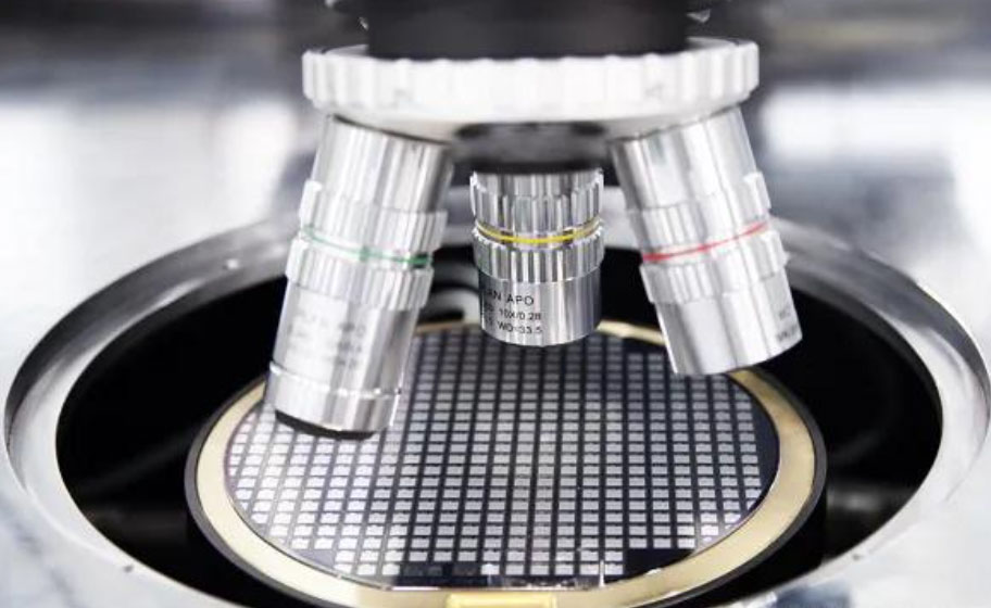
A wafer surface acts like a mirror. Light hits it, and most of it reflects away. The camera receives very little. If the light angle is wrong, the image is either completely dark or completely washed out — defect information is lost entirely.
Heat is another problem. Wafer inspection typically happens in cleanrooms, where temperature fluctuations affect measurement accuracy. Traditional halogen lamps generate significant heat — local temperature rise near the wafer can interfere with inspection results.
Coaxial fiber optic illumination is the most common approach in wafer inspection. Light is projected vertically from directly above the lens, and the reflected light returns along the same path into the camera — essentially "seeing" the true front-surface reflection of the wafer. Coaxial illumination eliminates angled shadows, making surface defects clearly visible in a uniform bright field.
Dark-field ring fiber takes a different approach. Light hits at a steep angle from the side. Flat surfaces reflect light away from the camera. Only raised defects scatter light into the lens. Defects "light up" against a dark background with extremely high contrast — ideal for detecting micro-particles and shallow scratches.
Cold light is equally important. Hecho‘s S5000 series LED cold light sources use a light-heat separation design. Heat stays at the source. The output end emits virtually no thermal radiation. The wafer doesn’t heat up from illumination, and measurement results stay stable.
Wafer inspection places specific demands on fiber uniformity and spectral characteristics. Quartz fiber offers low transmission loss and broad spectral range for applications requiring specific wavelengths. Glass fiber is cost-effective for standard visible-light inspection. Ring fiber optic light guides and coaxial fiber are the most commonly used configurations in wafer inspection.
Hecho Technology offers ring, coaxial, and linear fiber optic light guides in glass and quartz — with customizable inner diameter, outer diameter, and output angle based on wafer size, inspection wavelength, and machine space constraints.
If you‘re selecting an illumination solution for wafer inspection equipment, contact the Hecho technical team.
About Nanjing Hecho Technology Co., Ltd.
Hecho Technology focuses on optical transmission solutions for medical, industrial, and scientific applications. Products include plastic optical fiber, glass fiber, quartz fiber, fiber bundles, light guides, and sensors, with OEM/ODM customization available.
Website: www.gohecho.cn | Email: sales@gohecho.cn | Tel: (025)52374096


 IPv6 network supported
 English
 简体中文
简体中文